Co-Packaged Optics and Silicon Photonics for GPU Data Center Interconnects
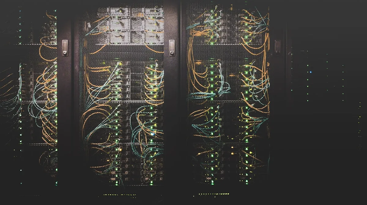
The bandwidth demands of AI training clusters are outpacing the capabilities of traditional pluggable optical transceivers. A single NVIDIA B200 GPU generates up to 1.8 Tbps of network traffic during distributed training, and a rack of eight GPUs requires over 14 Tbps of aggregate switching capacity. At these densities, the electrical interconnects between switch ASICs and front-panel transceiver cages become the primary bottleneck -- consuming more power than the optical transmission itself and limiting the port density that a switch can support.
Co-packaged optics (CPO) and silicon photonics represent the most significant architectural shift in data center networking since the transition from copper to fiber. By integrating optical engines directly into switch and processor packages, these technologies eliminate the electrical bottleneck, reduce interconnect power by 30-50%, and enable bandwidth densities that pluggable optics cannot physically achieve. For GPU data center operators planning infrastructure for the next generation of AI hardware, understanding these technologies is essential for making sound investment decisions today.
The Electrical Bottleneck Problem
To understand why co-packaged optics matter, it helps to trace the data path in a traditional switch. An InfiniBand or Ethernet switch ASIC sits at the center of a printed circuit board (PCB). Electrical signals travel from the ASIC through PCB traces, across connectors, and into front-panel transceiver cages (QSFP-DD or OSFP slots). These electrical traces are typically 15-30 centimeters long.
At low data rates (10-25 Gbps per lane), this electrical path works well. But at 100+ Gbps per lane -- the rates required for 400G and 800G ports -- the electrical signal degrades severely over even short distances. The high-frequency signals experience insertion loss (signal weakening), crosstalk (interference between adjacent traces), and impedance discontinuities at connectors and via transitions. Compensating for this degradation requires power-hungry SerDes (serializer/deserializer) circuits, retimers, and signal conditioning components.
Power Breakdown: Where the Watts Go
In a 51.2 Tbps switch using 800G pluggable optics, the power budget breaks down approximately as follows:
| Component | Power (Watts) | Percentage |
|---|---|---|
| Switch ASIC (switching logic) | ~300W | 25% |
| ASIC SerDes (electrical I/O) | ~350W | 29% |
| Pluggable transceivers (64x 800G) | ~450W | 38% |
| PCB power delivery, fans, misc | ~100W | 8% |
| Total | ~1,200W | 100% |
The SerDes and transceivers together consume 67% of the total switch power -- and they are not doing any switching. They are merely moving data between the ASIC and the optical fiber. In a GPU cluster with hundreds of switches, this represents hundreds of kilowatts consumed by signal conditioning alone, directly increasing PUE and energy costs.
How Co-Packaged Optics Work
Co-packaged optics eliminate the long electrical path by placing optical engines directly adjacent to -- or on top of -- the switch ASIC within the same package substrate. The electrical signals travel less than 5 millimeters from the ASIC to the optical transmitter, compared to 15-30 centimeters in a pluggable configuration. This dramatically shorter path requires far less signal conditioning power and supports higher data rates per lane.
Architecture Components
A CPO-based switch package contains several key components:
- Switch ASIC: The core switching silicon, functionally identical to current generation ASICs but with modified I/O designed for short-reach electrical connections to co-packaged optical engines rather than long-reach connections to front-panel transceivers.
- Optical engine chiplets: Small photonic integrated circuits (PICs) placed around the perimeter of the ASIC on the package substrate. Each optical engine converts electrical signals to optical signals (and vice versa) using silicon photonics modulators and photodetectors. A 51.2 Tbps switch might contain 16-32 optical engine chiplets.
- Fiber attachment: Optical fibers connect directly to the package through fiber array units (FAUs) that align each fiber to its corresponding waveguide on the optical engine. This eliminates front-panel transceiver cages entirely -- fibers exit the package directly.
- Package substrate: An advanced multi-layer substrate (typically organic or silicon interposer) that provides the electrical interconnects between the ASIC and optical engines, power delivery, and thermal management pathways.
Silicon Photonics: The Enabling Technology
Silicon photonics makes CPO economically viable by fabricating optical components using standard CMOS semiconductor manufacturing processes. Instead of building optical components from exotic materials (indium phosphide, gallium arsenide) in specialized facilities, silicon photonics creates waveguides, modulators, multiplexers, and (with hybrid integration) laser sources on standard silicon wafers in existing semiconductor fabs.
The key silicon photonic components in a CPO optical engine include:
- Silicon waveguides: Light channels etched into silicon-on-insulator (SOI) wafers that guide photons with low loss. The high refractive index contrast between silicon (n=3.48) and silicon dioxide (n=1.45) allows extremely compact waveguides -- bending radii under 10 micrometers -- enabling dense integration.
- Mach-Zehnder modulators: Silicon structures that encode data onto light by changing the refractive index of one arm of an interferometer through carrier injection or depletion. These modulators operate at 100+ Gbps per lane and are the primary data encoding mechanism in silicon photonic transmitters.
- Germanium photodetectors: Germanium (epitaxially grown on silicon) absorbs 1310nm and 1550nm light and converts photons to electrical current. Germanium photodetectors achieve bandwidths exceeding 100 GHz, sufficient for current and next-generation data rates.
- Wavelength-division multiplexing (WDM) components: Ring resonators, arrayed waveguide gratings, and Echelle gratings that combine or separate multiple wavelengths of light. WDM allows 4, 8, or 16 data channels to share a single fiber, multiplying bandwidth per fiber port.
- Hybrid-integrated laser sources: Silicon cannot efficiently emit light, so III-V semiconductor lasers (typically indium phosphide) are bonded or attached to the silicon photonic chip. These lasers provide the continuous-wave light that modulators then encode with data.
Performance Advantages for GPU Clusters
CPO provides three primary advantages for AI training infrastructure:
Power Reduction
By eliminating long electrical traces and the associated SerDes power, CPO reduces the per-port power consumption of optical I/O by 30-50%. For a 51.2 Tbps switch, this translates to approximately 300-400W of power savings -- reducing total switch power from ~1,200W to ~800W. In a GPU cluster with 64 spine and leaf switches, the aggregate savings reaches 20-25 kW. With power density as the primary constraint in AI data centers, this per-switch power reduction directly translates to more GPU compute capacity within the same power envelope.
Bandwidth Density
Pluggable transceivers are physically large: an OSFP module is 22.6mm wide and 107.8mm deep. A 2U switch faceplate can accommodate at most 64 OSFP ports. CPO eliminates front-panel transceivers entirely, because fibers connect directly to the package. This means the switch faceplate is no longer the bandwidth bottleneck -- the limiting factor becomes the ASIC's switching capacity and the fiber count. Future CPO switches could support significantly more optical ports than pluggable designs, enabling denser network fabrics with fewer switch tiers.
Reach and Signal Integrity
With CPO, the optical signal is generated within millimeters of the ASIC, so the signal enters the fiber at full strength without degradation from PCB traces. This improves reach (how far the signal can travel through fiber without amplification) and reduces bit error rates. For intra-data-center distances (typically under 2 km), CPO optical links can achieve lower error rates than pluggable optics, reducing the need for forward error correction (FEC) overhead and improving effective throughput.
Impact on Data Center Physical Design
CPO does not simply replace transceiver modules -- it fundamentally changes how data center infrastructure must be designed and operated.
Fiber Management Revolution
In a pluggable optics environment, fibers terminate at front-panel transceiver cages. When a transceiver fails, an operator unplugs the fiber, swaps the transceiver, and reconnects. With CPO, fibers are permanently attached to the switch package. This means:
- Pre-installed fiber infrastructure: All fiber runs must be installed and tested before the switch is deployed. Changes to the fiber topology after deployment require switch removal.
- Higher fiber counts per switch: CPO switches may use hundreds of individual fibers (or fiber ribbons) per package, compared to the 64-128 fibers (in duplex LC or MPO connectors) used by pluggable switches. Fiber tray and pathway capacity must increase accordingly.
- Structured cabling becomes critical: Because fibers cannot be easily reconnected, the initial cabling design must account for all possible future configurations. Over-provisioning fiber pathways and using high-density fiber management systems (MTP/MPO with 16-32 fibers per connector) becomes essential.
Thermal Design Changes
Pluggable transceivers generate heat at the switch faceplate, which is removed by front-to-back airflow through the switch chassis. CPO concentrates the heat generation at the package level -- the optical engines are co-located with the ASIC on the same substrate, creating a more concentrated heat source. This requires:
- More sophisticated package-level thermal solutions (larger heatsinks, vapor chambers, or liquid cooling integration)
- Reduced faceplate heat load (since transceivers are eliminated), potentially simplifying rack-level airflow
- Overall lower total heat output per switch (due to the power savings), reducing cooling requirements
Serviceability Model Changes
The pluggable transceiver model provides operational flexibility: a failed transceiver can be replaced in minutes without disrupting other ports on the same switch. CPO changes this model significantly:
- Optical engine failure: If one optical engine in a CPO package fails, the entire switch package may need replacement. However, CPO designs typically include redundant optical channels, and silicon photonic reliability data shows lower failure rates than pluggable transceivers (fewer connectors, no mechanical insertion/removal wear).
- Fiber damage: A damaged fiber at the package attachment point may require switch replacement, whereas pluggable optics simply need a new patch cable. This makes fiber route protection and cable management more critical.
- Inventory simplification: CPO eliminates the need to stock multiple transceiver types (DR4, FR4, LR4 in various speeds and form factors). The optical capability is built into the switch, reducing spare parts inventory complexity.
Current Industry Status and Roadmap
As of mid-2026, the CPO ecosystem is advancing rapidly but production deployments remain limited:
Major Players
- Broadcom: Has demonstrated a CPO-based 51.2 Tbps Memory Fabric (CMF) switch ASIC with integrated silicon photonic optical engines. Broadcom's CPO platform uses an organic package substrate with optical engines placed around the ASIC perimeter, connecting to fiber via MTP/MPO connectors. Initial production shipments are expected in late 2027.
- NVIDIA: Has signaled CPO integration for future networking platforms beyond the current ConnectX and Spectrum series. NVIDIA's interest in CPO is driven by the bandwidth requirements of NVLink and InfiniBand at the 1.6 Tbps-per-port tier.
- Intel: Operates one of the most mature silicon photonics programs, with volume production of pluggable silicon photonic transceivers (100G-400G). Intel's CPO roadmap leverages its advanced packaging capabilities (EMIB, Foveros) to integrate optical engines with switch ASICs.
- Ayar Labs: A startup focused specifically on optical I/O chiplets that can be integrated into any processor or switch package. Ayar Labs' TeraPHY chiplet provides 1 Tbps of optical bandwidth in a compact chiplet form factor, designed for CPO integration.
- Ranovus: Developing multi-wavelength silicon photonic engines optimized for CPO integration, with an emphasis on 1.6 Tbps and 3.2 Tbps per-port data rates.
Timeline for Adoption
| Timeframe | Technology | Data Center Segment |
|---|---|---|
| 2024-2026 (current) | 800G pluggable (OSFP, QSFP-DD800) | All segments |
| 2027-2028 | First CPO switches (51.2T), 1.6T pluggable | Hyperscale cloud, largest AI clusters |
| 2028-2030 | CPO mainstream (102.4T switches) | Large enterprise, GPU colocation |
| 2030+ | CPO standard for high-bandwidth switches | Broad adoption |
What Data Center Operators Should Do Now
While CPO production deployments are 1-3 years away for most operators, infrastructure decisions made today will determine whether a facility can adopt CPO when it becomes available.
Fiber Infrastructure
Design fiber pathways and tray capacity for 2-3x the current fiber count per rack. CPO switches will require significantly more fibers per switch than pluggable designs. Install single-mode fiber (OS2) for all new runs -- CPO primarily uses 1310nm single-mode optics. Avoid over-reliance on multimode fiber for new installations, as multimode is not compatible with most CPO designs.
Power and Cooling Headroom
While CPO reduces per-switch power, the expectation is that operators will deploy denser networking (more switches, or higher-capacity switches) rather than simply pocketing the savings. Plan power capacity for the same or higher aggregate network power, with the understanding that CPO enables more bandwidth within that power budget. Ensure cooling solutions can handle the concentrated heat load of CPO packages.
Vendor Strategy
Track CPO development from multiple vendors. Broadcom, NVIDIA, and Intel have different approaches and timelines. Avoid designs that assume a specific CPO vendor or package format, because the physical interface standards (fiber connector types, fiber counts) are still being finalized by industry bodies. Build operational relationships with silicon photonics companies to ensure early access to engineering samples and design guidance.
Operational Readiness
CPO changes the maintenance model. Train fiber technicians on high-density fiber handling and MTP/MPO connector cleaning. Develop procedures for CPO switch replacement that include fiber route documentation (because fibers are permanently attached). Update spare parts strategies to account for full switch package replacement rather than individual transceiver swaps.
The UAE/GCC Opportunity
Data center operators in the UAE and GCC building new GPU cluster facilities have a unique advantage: they are designing greenfield infrastructure without legacy constraints. New facilities can incorporate CPO-ready fiber pathways, cooling architectures compatible with CPO thermal profiles, and power distributions designed for the networking densities that CPO enables.
Regional sovereign AI initiatives driving deployment of large-scale GPU clusters (1,000+ GPUs) will be among the first colocation environments outside hyperscale cloud to require the bandwidth densities that CPO addresses. Operators who invest in CPO-ready infrastructure now will be positioned to offer the highest-performance interconnect environments when these technologies enter production.
Future-Proof Your Data Center Networking
Rax designs GPU cluster infrastructure with future optical interconnect requirements in mind. Our facilities feature high-density fiber pathways, advanced cooling, and the power capacity to support next-generation networking technologies as they enter production.
Discuss Your Infrastructure Requirements